Glossary · PCIe
PCIe lanes explained. — How many you have. How many you actually need.
Your motherboard has more physical slots than your CPU has lanes to feed them. That's why populating slot 2 sometimes disables an M.2. Lane budgeting is the hidden constraint behind every "weirdly-specced" motherboard layout. Here's how the maths actually works.
- AM5 CPU lanes
- 24 + 4
- LGA1851 lanes
- 20 + 24
- TR PRO HEDT lanes
- 128
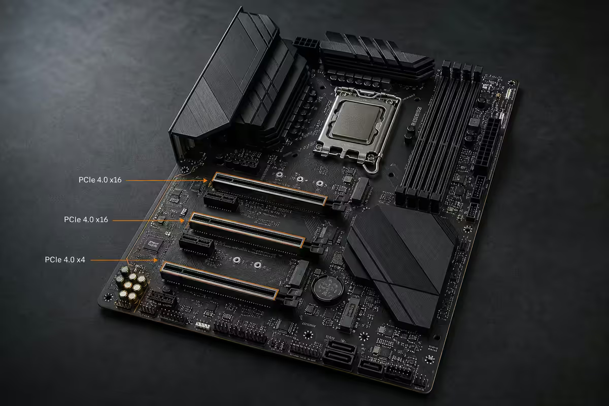
What is a PCIe lane?
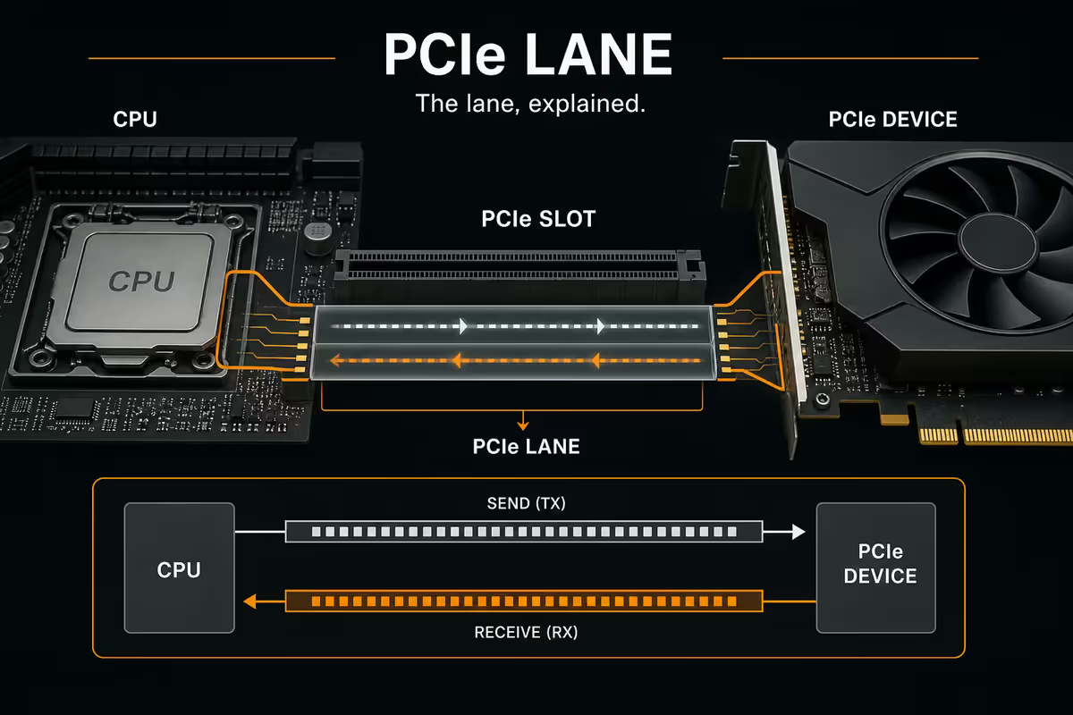
A PCIe lane is a single bidirectional data path between the CPU (or chipset) and an expansion device — a GPU, NVMe drive, USB4 controller, network card. Each lane has its own transmit pair and receive pair, running at a defined PCIe generation speed. Devices ask for a width (x1, x4, x8, x16) and a generation (Gen3, Gen4, Gen5), and the chipset assigns lanes from the available budget.
Generation matters as much as count. Each PCIe generation doubles the per-lane bandwidth. A single Gen5 lane delivers ~3.94 GB/s, the same as four Gen3 lanes. So fewer Gen5 lanes can serve faster devices than more Gen3 lanes — which is why modern lane budgets feel adequate despite seeming numerically small.
| Generation | Per-lane bandwidth | x16 total |
|---|---|---|
| PCIe Gen3 | ~0.98 GB/s | ~15.75 GB/s |
| PCIe Gen4 | ~1.97 GB/s | ~31.5 GB/s |
| PCIe Gen5 | ~3.94 GB/s | ~63 GB/s |
| PCIe Gen6 (server, 2026+) | ~7.88 GB/s | ~126 GB/s |
Lane counts by socket — what your motherboard actually has
Lane budget depends entirely on your CPU socket. Here's the 2026 reality for mainstream and HEDT platforms.
| Socket / CPU | CPU-direct lanes | Chipset adds |
|---|---|---|
| AMD AM5 (Ryzen 7000/9000) | 24 Gen5 + 4 Gen4 | ~12-16 Gen4 (X870) |
| AMD AM5 (mid-tier B650) | 24 Gen5 + 4 Gen4 | ~8 Gen4 (B650) |
| Intel LGA1851 (Core Ultra 200) | 16 Gen5 + 4 Gen4 | ~24 Gen4 (Z890) |
| Intel LGA1851 (B860 mid-tier) | 16 Gen5 + 4 Gen4 | ~14 Gen4 (B860) |
| AMD Threadripper 7000 (sTR5) | 48 Gen5 + 4 Gen4 | + additional 32+ via TRX50 |
| AMD Threadripper PRO 7000 (sWRX9) | 128 Gen5 lanes | HEDT-class abundance |
| Intel Xeon-W (LGA4677) | 112 Gen5 lanes | Workstation tier |
For a typical gaming or creator build, AM5 and LGA1851 mainstream platforms deliver dramatically more lane budget than you'll consume. The exception: workstation builds with multiple GPUs, NVMe RAID arrays or specialised capture / NIC cards.
CPU lanes vs chipset lanes — why the difference matters
Not all PCIe lanes are equal. The difference between CPU-direct lanes and chipset-fed lanes is where latency and bandwidth bottlenecks hide.
CPU-direct lanes connect straight from the processor's I/O die to the device — no intermediary chip. Lowest latency, full bandwidth, used for the primary GPU slot (x16) and the primary M.2 NVMe slot (x4). This is the premium real estate on every motherboard.
Chipset lanes are routed through the platform chipset chip — X870 / B650 on AMD, Z890 / B860 on Intel. The chipset itself connects to the CPU through a 4-lane DMI (Intel) or Infinity Fabric (AMD) link, which becomes the shared bottleneck. Even if the chipset has 24 lanes hanging off it, all of those lanes' traffic has to squeeze through the ~16 GB/s link back to the CPU.
What this means in practice: a chipset-fed M.2 NVMe drive can hit its rated sequential speeds in isolation. But if you're simultaneously copying from another chipset-fed NVMe, downloading at 10 GbE through a chipset-fed NIC and running USB devices all through the chipset, the aggregate traffic saturates the chipset link and everything slows. CPU-direct lanes never share with this traffic.
Lane sharing — the silent gotcha
Most motherboards have more physical slots than the chipset has independent lanes to feed. Manufacturers solve this with lane sharing — populating one slot disables or reduces another.
Common sharing scenarios on mid-tier 2026 boards:
- Second PCIe x16 slot shares lanes with M.2_3 — populating the secondary slot drops M.2_3 to "not present" in BIOS.
- SATA ports 5 and 6 share with M.2_2 — installing a Gen4 NVMe in M.2_2 disables two SATA ports.
- USB4 controller pulls 4 chipset lanes — on boards with USB4, this dedicated allocation reduces lanes available for other chipset devices.
- Primary x16 slot drops to x8 when slot 2 is x8 — common on workstation boards designed for dual-GPU configurations, less so on gaming boards.
How to plan around sharing. Open the motherboard PDF manual, find the PCIe topology table (usually in the specifications section, page 3-5). It explicitly lists which slots share lanes with which other slots. Map your intended hardware against the table before purchase. The MSI X870E Carbon WiFi, Asus ROG X870E Hero and Gigabyte X870E Aorus Master all have published topology diagrams that make this clear.
GPU lane needs — x16, x8, and the gaming truth
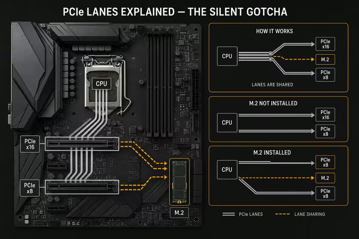
Every modern dGPU takes a physical x16 slot — that's the connector shape. Whether the slot operates at x16 or x8 depends on the motherboard and what else is populated.
The gaming benchmark reality: RTX 5070, RTX 5080 and even RTX 5090 lose only 1-3% average framerate when running at Gen5 x8 versus Gen5 x16. The gap is similarly tiny between Gen4 x16 and Gen4 x8. Games are rarely bandwidth-bound at the PCIe level — they're bound by VRAM, memory bandwidth and shader throughput.
When the GPU PCIe width actually matters:
- AI / ML compute — large model batch loads can be PCIe-bound. x16 vs x8 difference is measurable for LLM inference and Stable Diffusion training.
- Old GPU on modern board — an RTX 2080 dropped to Gen3 x8 (legacy slot) loses 5-8% performance. New GPUs at Gen5 x8 don't see this.
- SLI / multi-GPU — splitting the primary x16 into x8/x8 for dual GPUs is standard on workstation boards but largely irrelevant for gaming in 2026 (SLI is functionally dead).
- 8K video / RAW playback — niche workflow where GPU PCIe bandwidth genuinely matters.
NVMe and USB4 — where lanes actually disappear
For most builders, NVMe drives are the largest consumer of lane budget after the GPU. Each PCIe Gen4 or Gen5 NVMe drive takes 4 lanes — three or four drives quickly add up.
NVMe lane consumption on an AM5 X870E board:
- M.2_1 (CPU-direct, Gen5 x4) — 4 CPU Gen5 lanes
- M.2_2 (chipset-fed, Gen4 x4) — 4 chipset Gen4 lanes
- M.2_3 (chipset-fed, Gen4 x4) — 4 chipset Gen4 lanes
- M.2_4 (chipset-fed, Gen4 x4) — 4 chipset Gen4 lanes (often shares with PCIe slot 2 or SATA)
Three or four NVMe drives is the practical ceiling for a mainstream board without sacrificing other slots. If you need 5+ NVMe drives for video editing scratch space, Plex media storage, or NVMe RAID for production work, HEDT (Threadripper PRO) becomes the right answer — its 128 CPU-direct lanes can feed 8-12 NVMe drives at full bandwidth simultaneously.
USB4 / Thunderbolt 4 consumes 4 lanes per port. AM5 X870 chipsets include native USB4; B650 boards usually skip it (the lane budget is too tight). If you're planning an eGPU dock, a Thunderbolt audio interface or a multi-monitor dock, USB4 / TB4 lane allocation matters and you want X870 or Z890 rather than B650 or B860.
When HEDT lanes actually matter
HEDT (High-End DeskTop) platforms — AMD Threadripper PRO 7000 and Intel Xeon-W — bring 100+ PCIe lanes directly from the CPU. For almost every builder, that's gloriously unnecessary. But for the few with specific workloads, mainstream lane budget physically cannot serve the build.
HEDT lane abundance is necessary when:
- Multi-GPU compute farms — dual or quad RTX 5090s for LLM inference, Stable Diffusion training, scientific compute. Each GPU wants x16; mainstream platforms only have one x16 slot.
- Multi-NVMe RAID arrays — six to twelve NVMe drives in RAID for video editing scratch (cinema-grade 8K editing genuinely needs this).
- Production video capture — multiple Blackmagic DeckLink cards, SDI capture interfaces, broadcast-tier I/O cards. Each capture card eats x4 or x8.
- Workstation NICs — 25 GbE and 100 GbE network cards for production storage rendering, datacentre uplinks.
- Massive ECC RAM requirements — 256GB+ ECC memory, which only HEDT platforms officially support in registered DIMMs.
If your build doesn't fit one of these workloads, you don't need HEDT — and you'll pay a 3-5× price premium for lane budget you'll never consume. The Ryzen 9 9950X3D on a mainstream X870E delivers more single-thread performance than a Threadripper PRO at half the platform cost.
Key takeaways
- A PCIe lane is one bidirectional data path. Generation doubles bandwidth each version — Gen5 = 4× Gen3.
- AM5 = 24+4 CPU lanes + chipset. LGA1851 = 20 CPU + 24 chipset. HEDT = 100+ direct.
- CPU-direct lanes are lower latency. Chipset lanes share a 16 GB/s link upstream.
- Lane sharing is real — populating slot 2 often disables M.2_3. Read the topology table.
- GPU x8 vs x16 hurts 1-3% in gaming. Mostly irrelevant outside AI workloads.
- HEDT only matters for multi-GPU, multi-NVMe RAID or production capture builds.
Frequently asked questions
How many PCIe lanes does my CPU have?
It depends on the socket. AMD AM5 (Ryzen 7000/9000) gives 24 usable PCIe Gen5 lanes from the CPU plus 4 Gen4 lanes for the chipset link, with another ~16 Gen4 lanes from the chipset. Intel LGA1851 (Core Ultra 200 series) gives 20 lanes from the CPU (16 Gen5 + 4 Gen4) plus another 24 Gen4 lanes from the Z890 chipset. AMD Threadripper PRO 7000 has 128 PCIe Gen5 lanes directly from the CPU — HEDT-class lane abundance.What is the difference between CPU lanes and chipset lanes?
CPU lanes connect directly to the processor — lowest latency, fastest bandwidth, used for the primary GPU slot (x16) and the primary M.2 NVMe slot. Chipset lanes go through the PCH (Intel) or FCH (AMD) chipset chip, which is connected to the CPU by a 4-lane DMI / Infinity Fabric link. Chipset lanes serve secondary M.2 slots, secondary PCIe slots, SATA, USB, networking and audio. The chipset link itself is the bottleneck — total chipset bandwidth maxes out around 16 GB/s aggregate.Why does my second PCIe slot disable my M.2 slot?
Lane sharing. Most B650, X670, B860 and Z890 motherboards have more physical slots than the chip can independently feed, so the BIOS shares lanes between secondary PCIe slots and M.2 slots. Populating slot 2 with an x4 device (capture card, AIC, NIC) often disables one of the M.2 slots. The motherboard manual's PCIe topology table lists every shared lane — read it before buying.How many PCIe lanes does an RTX 5090 actually use?
The RTX 5090 uses PCIe Gen5 x16 — sixteen Gen5 lanes. In practice, it'll perform within 1-3% of full speed on Gen5 x8 or Gen4 x16, and most games show no difference at all between Gen5 x16 and Gen4 x8. The x16 spec matters for niche workloads like AI compute or 8K video editing where the GPU is genuinely bandwidth-bound.Do I need a HEDT platform for multiple NVMe drives?
No. AM5 and LGA1851 boards support 2-4 M.2 NVMe drives without HEDT pricing. HEDT (Threadripper PRO, Xeon-W) only becomes necessary when you need 4+ NVMe drives running at full bandwidth simultaneously — for example, NVMe RAID arrays for video editing scratch disks, or workstations with dual GPUs plus multiple capture cards. For a typical creator or gamer, AM5 / LGA1851 lane budget is plenty.Will running my GPU at x8 instead of x16 hurt gaming performance?
Almost never. Modern GPUs from RTX 4070-class up to RTX 5090 lose 1-3% average framerate on Gen5 x8 versus Gen5 x16. The gap is similar between Gen4 x16 and Gen4 x8. Where x8 hurts more is older GPUs on Gen3 x8, or specific GPU compute workloads that hammer the PCIe bus. For 99% of gaming, x8 versus x16 is a non-issue.What is USB4 and how many lanes does it use?
USB4 is the open-standard cousin of Thunderbolt 4, providing 40 Gbps per port with DisplayPort alt-mode, Power Delivery and tunnelled PCIe. Each USB4 / Thunderbolt 4 port consumes 4 PCIe lanes from the system lane budget. AM5 X870 chipsets include native USB4 controllers; cheaper B650 boards usually skip it. If you're planning an eGPU dock or 4K dual-monitor setup, USB4/Thunderbolt 4 with its dedicated lane allocation matters.How do I check my actual PCIe lane allocation in Windows?
GPU-Z shows the GPU's current lane width and PCIe generation in real time — Gen5 x16, Gen4 x8, etc. HWiNFO64 shows every PCIe device and which lanes it occupies. CPU-Z's mainboard tab reveals chipset link status. The most useful is the motherboard manual's PCIe topology diagram, which maps every slot's lane source (CPU vs chipset) and any sharing rules. Read this before building, not after.
Get the Evetech app
Exclusive app-only prices, daily flash sales, and free delivery on orders over R4,000 — download the app and start saving.