GPU Spec Sheet Decoder
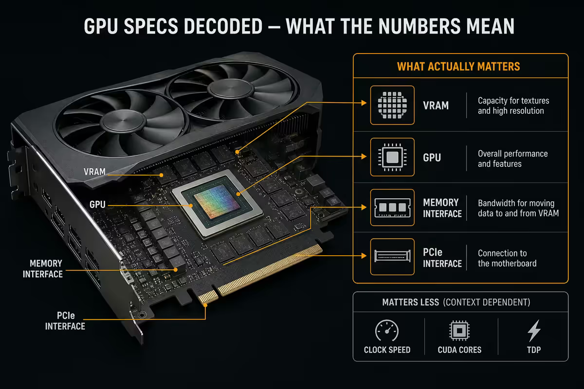
GPU specs decoded. — What the numbers actually mean.
Every retailer spec sheet throws fifteen acronyms at you. Most of them barely move the frame rate. Here's which ones matter, which ones don't, and how to read between the lines on a GPU listing.
- specs decoded
- 15+
- that actually matter
- 3
- read time
- 8 min
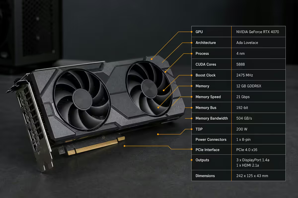
VRAM — the size of your texture wallet
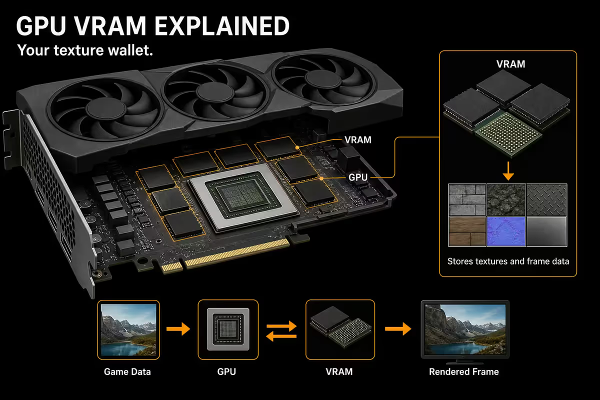
VRAM (Video RAM) is dedicated memory soldered directly onto the GPU board. It holds textures, frame buffers, shadow maps, mesh data and any asset the GPU needs to reach instantly. Modern cards use GDDR6, GDDR6X or GDDR7 — newer generations are faster, but the headline number on a spec sheet is always the size.
VRAM does not make games faster. What it does is set a hard ceiling on how much detail you can run. When a game wants more memory than the card has, you get one of three outcomes: textures pop in late, frame times stutter as the system swaps assets over PCIe, or the game outright crashes. None of those are fun at 11pm in a ranked match.
| Resolution | Practical floor | Comfortable |
|---|---|---|
| 1080p — esports | 6 GB | 8 GB |
| 1080p — modern AAA | 8 GB | 10-12 GB |
| 1440p — high textures | 10 GB | 12 GB |
| 1440p — ray tracing on | 12 GB | 16 GB |
| 4K — AAA + RT | 16 GB | 20-24 GB |
| VR / content creation | 16 GB | 24 GB + |
Memory bus and bandwidth — the spec marketers hide
Memory bus width is how wide the highway between the GPU die and VRAM chips is, measured in bits — usually 128, 192, 256, 320 or 384. Memory bandwidth is the actual GB per second the GPU can move, calculated as bandwidth = bus width × effective speed ÷ 8.
Bus width is where mid-range cards get quietly hamstrung. A 128-bit card with 16 GB of VRAM looks impressive on a Takealot listing — but it will choke at 1440p ray tracing because there's not enough bandwidth to feed the cores. A 256-bit card with 12 GB will out-perform it every time at the same resolution.
When two cards in the same tier have meaningfully different bus widths, the narrower one is almost always the worse buy. The exception is cards designed specifically for 1080p — where 128-bit is sized correctly for the workload.
CUDA cores, stream processors, RT cores and Tensor cores
CUDA cores (NVIDIA) and stream processors (AMD) are the general-purpose shader cores doing the bulk of the rendering work — vertex transforms, pixel shading, post-processing. More is better within the same architecture, useless to compare across architectures.
An RTX 3060 has 3 584 CUDA cores. An RTX 5060 has 4 608. The 5060 is faster per core because the architecture improved — so even matched core counts wouldn't be matched performance. Never compare CUDA cores from one generation to the next or from NVIDIA to AMD.
RT cores are dedicated hardware for ray-triangle intersection — the core operation in ray tracing. Generation matters more than count: a 4th-gen RT core is roughly 2.5× faster than a 1st-gen one. Tensor cores accelerate AI workloads including DLSS upscaling, frame generation, and increasingly the new neural-rendering shaders. These are why NVIDIA cards punch above their raw raster spec in supported games.
AMD's equivalent is "Ray Accelerators" and "AI Accelerators" — same function, different naming. Don't try to map RA counts to RT core counts; they're not equivalent units.
TGP, TBP and TDP — what the card pulls
TGP (Total Graphics Power, NVIDIA) and TBP (Total Board Power, AMD) are the headline power draw of the entire card under sustained load. TDP is the older general term and still appears on some listings — treat it as approximately the same number.
TGP drives three real-world consequences: PSU requirement, case heat, and noise. A 320 W TGP card in a closed, poorly-ventilated case will run loud and eventually thermal-throttle in our 32°C Joburg summers — even more so when load shedding ends and your UPS-backed system runs hot all afternoon.
| TGP / TBP | Minimum PSU | Cooling notes |
|---|---|---|
| 120-180 W (entry) | 550 W | Any mid-tower, two fans fine |
| 200-260 W (mid) | 650-750 W | Three intake fans, mesh front |
| 280-320 W (high) | 850 W | High airflow case, front-mesh mandatory |
| 350-450 W (flagship) | 1000 W + | Front mesh + top exhaust + 140mm fans |
Base and boost clock
Base clock is the minimum guaranteed frequency the GPU runs at under sustained load. Boost clock is the top frequency it'll target if thermal and power budgets allow. Real-world clocks land somewhere in between and depend on cooling, case temperature, power limit and the specific workload.
Where boost clock genuinely matters: comparing partner cards. ASUS, MSI, Gigabyte and Galax all build cards using the same NVIDIA reference die. A 100-150 MHz boost difference between models tells you which one is tuned more aggressively, which is generally a proxy for cooler quality. The tradeoff is usually noise and power.
What boost clock does not tell you: how the card actually performs. Two cards with the same boost clock can be 10% apart in benchmarks because of cooling differences, power limits and silicon lottery.
FP32 TFLOPS — the most overrated single number
FP32 TFLOPS (trillion 32-bit floating point operations per second) is the theoretical peak compute the card can achieve. The formula is cores × boost clock × 2 ÷ 1 000 000. It looks scientific. It is largely useless as a gaming predictor.
Why? Because gaming performance depends on architecture efficiency, memory bandwidth, cache size, driver tuning, RT and Tensor core counts and the specific workload. Two cards with identical TFLOPS can be 20% apart in actual games. AMD cards typically post higher TFLOPS than NVIDIA equivalents because their architecture trades efficiency for raw compute — but NVIDIA still wins most benchmarks.
Use TFLOPS as one rough data point when comparing within a single brand and generation. Anywhere else, look at benchmarks, not the marketing slide.
TMUs, ROPs and PCIe — the back-of-spec-sheet specs
TMUs (Texture Mapping Units) sample and filter textures. ROPs (Render Output Units) handle the final pixel writes including blending, anti-aliasing and writes to the frame buffer. Both scale with the GPU tier — you don't tune for either directly.
Where ROPs occasionally matter is at very high resolutions. A card with too few ROPs for its compute will bottleneck at 4K with heavy anti-aliasing. This shows up in benchmarks as much lower 4K performance relative to 1440p. If a card looks anomalously weak at 4K despite strong 1440p numbers, ROP count is often the culprit.
PCIe lanes and generation: in 2026, PCIe 4.0 × 16 is the floor for any modern GPU. PCIe 5.0 × 16 is the new standard on AM5 and LGA1851 boards. The real-world difference between PCIe 4.0 and 5.0 for gaming is under 2% — even on a flagship card. PCIe 5.0 matters more for content workloads, direct-storage assets, and edge cases where the GPU streams unusually large data sets.
Watch out for entry GPUs that ship with PCIe x8 instead of x16. On a PCIe 4.0 motherboard, this halves your effective bandwidth. On a PCIe 3.0 motherboard (older Ryzen 3000-series or 10th-gen Intel), the impact compounds and you can lose 8-15% performance.
After shipping <strong>200,000+ custom PCs</strong> from our Centurion warehouse, the most common GPU mistake we see customers make is buying the card with the largest VRAM number in their budget — even when the bus width is too narrow to feed it. A 12 GB card on a 192-bit bus will out-perform a 16 GB card on a 128-bit bus at every resolution above 1080p. <strong>VRAM size is the headline; bandwidth is the verdict.</strong> Always check both numbers before committing.
Behind the Build · From our Centurion floor
What actually matters when shopping
The five numbers that decide your frame rate:
- VRAM size — sets your texture and resolution ceiling.
- Memory bus width — caps how much of that VRAM the GPU can actually use.
- CUDA core / stream processor count — within the same generation, scales linearly with performance.
- Boost clock — for partner-card comparisons within the same model line.
- TGP — tells you the PSU, the case cooling and the noise level you'll live with.
The numbers you can mostly ignore:
- FP32 TFLOPS — use it only inside one brand and generation.
- TMU and ROP counts — scale with tier, never the deciding factor.
- RGB zone count — has no effect on rendering.
- Display output count beyond 3 — most builds use 1-2 monitors.
- PCIe generation — 4.0 vs 5.0 is under 2% in games.
Key takeaways
- 01.
VRAM size and bus width
VRAM size sets the ceiling; bus width sets how fast you can reach it. Both numbers matter together. - 02.
Core counts are architecture-specific
CUDA cores and stream processors are not cross-comparable across architectures or brands. - 03.
TGP picks your build requirements
TGP picks your PSU, your case airflow and your noise budget — read it before you commit. - 04.
FP32 TFLOPS is theoretical
FP32 TFLOPS is theoretical peak compute — use benchmarks for real performance. - 05.
PCIe generation is negligible in games
PCIe 4.0 vs 5.0 is under 2% in games. Don't pay a premium chasing this number.
Frequently asked questions
What does VRAM mean and how much do I need?
VRAM is the dedicated memory on the GPU holding textures and frame buffers. 8 GB minimum at 1080p, 12 GB sweet spot at 1440p, 16 GB+ for 4K and ray tracing.What is memory bandwidth and why does it matter?
Memory bandwidth is how fast the GPU moves data in and out of VRAM (GB/s). It's calculated as bus width × speed ÷ 8 and is often the real bottleneck at higher resolutions.What are CUDA cores, stream processors, RT cores and Tensor cores?
CUDA cores (NVIDIA) and stream processors (AMD) are shader cores. RT cores accelerate ray tracing. Tensor cores accelerate AI workloads like DLSS. Not comparable across brands or generations.What is TGP, TBP and TDP on a GPU?
All three describe the card's power draw under load. TGP/TBP is what NVIDIA and AMD use today; TDP is the older term. It drives your PSU choice and case cooling needs.What's the difference between base clock and boost clock?
Base is the guaranteed minimum under load; boost is the maximum the card targets when thermal and power budgets allow. Real-world clocks land between the two.What are FP32 TFLOPS and is it a meaningful spec?
Theoretical peak compute calculated from cores × clock × 2. Useful only inside one brand and generation — don't compare across architectures.What are TMUs and ROPs on a GPU?
TMUs handle texture sampling; ROPs handle final pixel writes. Both scale with the GPU tier. They rarely decide a purchase but can explain weak 4K performance.Does PCIe 5.0 matter for a GPU?
For gaming in 2026, PCIe 4.0 x16 is enough. PCIe 5.0 matters more for content creation and direct-storage workloads — under 2% in real games.
Get the Evetech app
Exclusive app-only prices, daily flash sales, and free delivery on orders over R4,000 — download the app and start saving.